- 您现在的位置:买卖IC网 > Sheet目录2008 > MAX1184ECM+TD (Maxim Integrated Products)IC ADC 10BIT 20MSPS DL 48-TQFP
MAX1184
Dual 10-Bit, 20Msps, 3V, Low-Power ADC with
Internal Reference and Parallel Outputs
2
_______________________________________________________________________________________
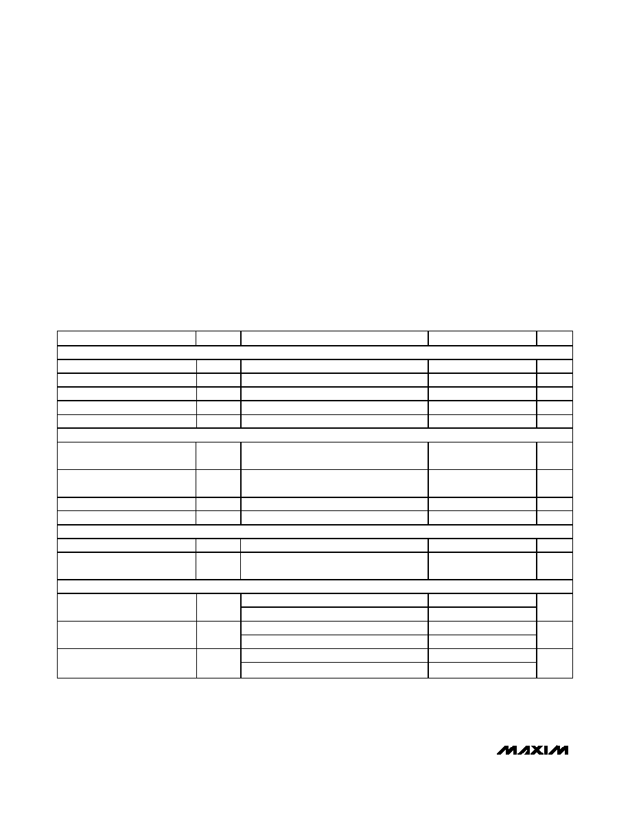
ABSOLUTE MAXIMUM RATINGS
ELECTRICAL CHARACTERISTICS
(VDD = 3V, OVDD = 2.5V, 0.1F and 1.0F capacitors from REFP, REFN, and COM to GND; REFOUT connected to REFIN through a
10k
resistor, VIN = 2VP-P (differential with respect to COM), CL = 10pF at digital outputs (Note 1), fCLK = 20MHz, TA = TMIN to TMAX,
unless otherwise noted. Typical values are at TA = +25°C.) (Note 2)
Stresses beyond those listed under “Absolute Maximum Ratings” may cause permanent damage to the device. These are stress ratings only, and functional
operation of the device at these or any other conditions beyond those indicated in the operational sections of the specifications is not implied. Exposure to
absolute maximum rating conditions for extended periods may affect device reliability.
VDD, OVDD to GND...............................................-0.3V to +3.6V
OGND to GND.......................................................-0.3V to +0.3V
INA+, INA-, INB+, INB- to GND ...............................-0.3V to VDD
REFIN, REFOUT, REFP, REFN, CLK,
COM to GND ..........................................-0.3V to (VDD + 0.3V)
OE, PD, SLEEP, T/B, D9A–D0A,
D9B–D0B to OGND .............................-0.3V to (OVDD + 0.3V)
Continuous Power Dissipation (TA = +70°C)
48-Pin TQFP-EP (derate 30.4mW/°C above
+70°C).......................................................................2430mW
Operating Temperature Range ...........................-40°C to +85°C
Junction Temperature ......................................................+150°C
Storage Temperature Range .............................-60°C to +150°C
Lead Temperature (soldering, 10s) .................................+300°C
PARAMETER
SYMBOL
CONDITIONS
MIN
TYP
MAX
UNITS
DC ACCURACY
Resolution
10
Bits
Integral Nonlinearity
INL
fIN = 7.5MHz
±0.5
±1.5
LSB
Differential Nonlinearity
DNL
fIN = 7.5MHz, no missing codes guaranteed
±0.25
±1.0
LSB
Offset Error
<
±1
±1.8
% FS
Gain Error
0
±2
% FS
ANALOG INPUT
Differential Input Voltage
Range
VDIFF
Differential or single-ended inputs
±1.0
V
Common-Mode Input Voltage
Range
VCM
VDD/2
± 0.5
V
Input Resistance
RIN
Switched capacitor load
100
k
Input Capacitance
CIN
5pF
CONVERSION RATE
Maximum Clock Frequency
fCLK
20
MHz
Data Latency
5
Clock
Cycles
DYNAMIC CHARACTERISTICS
fINA or B = 7.5MHz, TA = +25°C
57.3
59.5
Signal-to-Noise Ratio
(Note 3)
SNR
fINA or B = 12MHz
59.4
dB
fINA or B = 7.5MHz, TA = +25°C
57
59.4
Signal-to-Noise and Distortion
(Note 3)
SINAD
fINA or B = 12MHz
59.2
dB
fINA or B = 7.5MHz, TA = +25°C
64
74
Spurious-Free Dynamic Range
(Note 3)
SFDR
fINA or B = 12MHz
72
dBc
发布紧急采购,3分钟左右您将得到回复。
相关PDF资料
MAX1186ECM+TD
IC ADC 10BIT 40MSPS DL 48-TQFP
MAX1187CCUI+
IC ADC 16BIT 135KSPS 28-TSSOP
MAX118EAI+
IC ADC 8BIT 1MSPS 28-SSOP
MAX1191ETI+T
IC ADC 8BIT 7.5MSPS DL 28-TQFN
MAX1192ETI+T
IC ADC 8BIT 22MSPS DL 28-TQFN
MAX1195ECM+TD
IC ADC 8BIT 40MSPS DL 48-TQFP
MAX1197ECM+TD
IC ADC 8BIT 60MSPS DL 48-TQFP
MAX1202AEPP+
IC ADC 12BIT 8CH 20-DIP
相关代理商/技术参数
MAX1184ECM-D
功能描述:模数转换器 - ADC RoHS:否 制造商:Texas Instruments 通道数量:2 结构:Sigma-Delta 转换速率:125 SPs to 8 KSPs 分辨率:24 bit 输入类型:Differential 信噪比:107 dB 接口类型:SPI 工作电源电压:1.7 V to 3.6 V, 2.7 V to 5.25 V 最大工作温度:+ 85 C 安装风格:SMD/SMT 封装 / 箱体:VQFN-32
MAX1184ECM-T
制造商:Maxim Integrated Products 功能描述:DUAL 10-BIT, 20MSPS, +3V, LOW-POWER ADC WITH - Tape and Reel
MAX1184ECM-TD
功能描述:模数转换器 - ADC RoHS:否 制造商:Texas Instruments 通道数量:2 结构:Sigma-Delta 转换速率:125 SPs to 8 KSPs 分辨率:24 bit 输入类型:Differential 信噪比:107 dB 接口类型:SPI 工作电源电压:1.7 V to 3.6 V, 2.7 V to 5.25 V 最大工作温度:+ 85 C 安装风格:SMD/SMT 封装 / 箱体:VQFN-32
MAX11850ETM+
功能描述:触摸屏转换器和控制器
RoHS:否 制造商:Microchip Technology 类型:Resistive Touch Controllers 输入类型:3 Key 数据速率:140 SPS 分辨率:10 bit 接口类型:4-Wire, 5-Wire, 8-Wire, I2C, SPI 电源电压:2.5 V to 5.25 V 电源电流:17 mA 工作温度:- 40 C to + 85 C 封装 / 箱体:SSOP-20
MAX11850ETM+T
功能描述:触摸屏转换器和控制器
RoHS:否 制造商:Microchip Technology 类型:Resistive Touch Controllers 输入类型:3 Key 数据速率:140 SPS 分辨率:10 bit 接口类型:4-Wire, 5-Wire, 8-Wire, I2C, SPI 电源电压:2.5 V to 5.25 V 电源电流:17 mA 工作温度:- 40 C to + 85 C 封装 / 箱体:SSOP-20
MAX11850GTM+
功能描述:触摸屏转换器和控制器
RoHS:否 制造商:Microchip Technology 类型:Resistive Touch Controllers 输入类型:3 Key 数据速率:140 SPS 分辨率:10 bit 接口类型:4-Wire, 5-Wire, 8-Wire, I2C, SPI 电源电压:2.5 V to 5.25 V 电源电流:17 mA 工作温度:- 40 C to + 85 C 封装 / 箱体:SSOP-20
MAX11850GTM+T
功能描述:触摸屏转换器和控制器
RoHS:否 制造商:Microchip Technology 类型:Resistive Touch Controllers 输入类型:3 Key 数据速率:140 SPS 分辨率:10 bit 接口类型:4-Wire, 5-Wire, 8-Wire, I2C, SPI 电源电压:2.5 V to 5.25 V 电源电流:17 mA 工作温度:- 40 C to + 85 C 封装 / 箱体:SSOP-20
MAX11850HTEVS+
功能描述:数据转换 IC 开发工具 RoHS:否 制造商:Texas Instruments 产品:Demonstration Kits 类型:ADC 工具用于评估:ADS130E08 接口类型:SPI 工作电源电压:- 6 V to + 6 V